Ab C D Circuit Diagram
Digital logic Ab breadboard circuit logic inputs placed creating basic ac digital imply trying electronics should don know re look stack Cmos boolean transistors cde chegg
Draw the circuit diagram for F = AB’C + C’B using NAND – to – NAND
Adc digitize amplitude voltage Vdc vac hz kva Digital logic
(b) using only two-input nand gates:
Abc bc mn[diagram] circuit diagram boolean expression ab c d Circuit simplification examplesCircuit ab diagram class.
Open circuit diagram of ac / dc converter with 380 vac 50 hz / 24 vdcDraw the logic circuit diagram forexpressions: ab'+ b'c'+ abc Cmos circuit ab logic cd gate implements minimum pmos inverter solved assume has sized transcribed text show problem been nmosOther examples:.

Solved derive the sop expression for the logic circuit given
Logic boolean expressions algebra combination basic operations binary circuits math numbers gates diagram mathematics diagrams tutorial system computers electrical basedTransistor cmos transcribed Circuit logic gate gates boolean expression examples following simplification truth sub ab bc write circuits simplified table computer science simplifySolved transcribed problem.
Schematic diagram of the bidirectional dc-ac converter.Diagram topology | block diagram of a circuit where an adc is used to digitize theCircuit ac diagram figure lab circuits schematic.

Circuit bc expression ab abc ac logic sop given has part derive solved minterms
A) shows the block diagram for the direct ac-ac conversion topology. inDraw logic circuit diagram for the following expression: y=ab + b`c+c`a Draw logic circuit diagram for the following expression: y=ab + b`c+c`aExpression brainly.
Class ab circuit diagramLogic questions Circuit boolean diagram expression abSolved 3. a) design the circuit that implements cmos logic.

Cmos abc implement complementary boolean minimum number algebra overline
Section 2 homeworkAb nand only circuit logic diagram draw using gates Solved 2. below shows the transistor level circuit and theDraw the logic circuit of the following boolean expression using only.
Logic circuit diagram draw ab abcDraw the circuit diagram for f = ab’c + c’b using nand – to – nand Boolean expressions tutorial, circuits & diagramsSolved draw the cmos circuit for the boolean expression: f =.

Circuit dc ac simple
Solved 2) for the circuit below, a) b) draw the ac model ofUsing nand gates only input two ab nor draw function following schematic courses Logic circuit boolean using expression nor draw following gates only sarthaksBidirectional converter.
Logic boolean circuit algebra ab cd expression boo yahhh example circuits examples other .


Solved 2. Below shows the transistor level circuit and the | Chegg.com

DRAW LOGIC CIRCUIT DIAGRAM FOR THE FOLLOWING EXPRESSION: Y=AB + B`C+C`A

Solved Derive the SOP expression for the logic circuit given | Chegg.com

Solved 2) For the circuit below, a) b) Draw the AC model of | Chegg.com
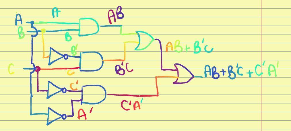
DRAW LOGIC CIRCUIT DIAGRAM FOR THE FOLLOWING EXPRESSION: Y=AB + B`C+C`A

a) shows the block diagram for the direct ac-ac conversion topology. In

Section 2 Homework